How far are 2D semiconductors from use in commercial logic chips?
In June 2026, imec, ASML and TSMC reported scaled transistors on 300mm wafers. The n-type devices used MoS2 and the p-type devices used WS2 or WSe2, at a 50nm contacted poly pitch. Imec describes the work as a 300mm test platform for studying 2D materials, not a product. The sources reviewed do not describe any commercial logic chip with a 2D channel, and they give no production date. The main gaps are contact resistance, especially for p-type devices, defects, growth of large uniform films and gate dielectrics.
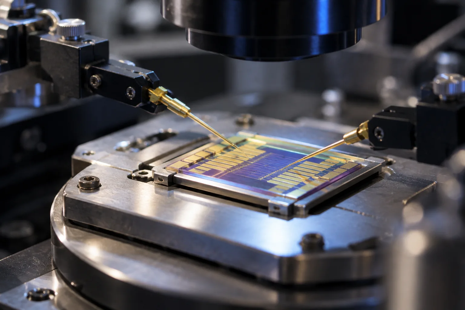
Getting closer. Prototypes exist, but not in real-world use.
Transistors with 2D channels have switched well in laboratories, and in June 2026 imec, ASML and TSMC reported nFETs and pFETs made on 300mm wafers at a 50nm contacted poly pitch. Those results are engineering prototypes on a test platform. No commercial logic chip with a 2D channel is described in the sources reviewed, and the reported yield figure has not been independently checked. The stage is therefore engineering prototype rather than pilot.
The tech tree
Everything recorded on Vrulum that this future needs, oldest foundations at the top and the goal at the bottom. Lines show what each step requires.
- 2026Scaled nFETs and pFETs on 300mm wafers at 50nm contacted poly pitchDone Unlocked.
- Date not recordedLab transistors with 2D channels switching wellDone Unlocked.
- Date not recordedUniform, large-area, single-crystal channel filmsIn progress Being researched.
- Date not recordedLow-resistance contacts for p-type devicesIn progress Being researched.
- Date not recordedDefect control and gate dielectrics suitable for productionIn progress Being researched.
- Date not recordedFoundry roadmap entry with a stated production dateNot started Locked.
- Date not recorded2D-channel logic chip in commercial productionNot started Locked.
- GoalComputer chips built from atom-thin materialsGoalRequires: 2D semiconductor electronics, Lab transistors with 2D channels switching well, Scaled nFETs and pFETs on 300mm wafers at 50nm contacted poly pitch, Uniform, large-area, single-crystal channel films, Low-resistance contacts for p-type devices, Defect control and gate dielectrics suitable for production, Foundry roadmap entry with a stated production date, 2D-channel logic chip in commercial production. Locked.
The road so far
2 of 7 steps done, 3 in progress.
- DoneLab transistors with 2D channels switching well
A 2025 review in Nano Letters reports CVD-grown MoS2 transistors with a subthreshold swing as low as 70 mV per decade and an on-off ratio up to 10^7. The review ties these figures to short-channel transistors with a single-crystal SrTiO3 gate dielectric. It also reports a WSe2 pFET with a contact resistance of 0.75 kΩ·μm, which it describes as a record-low value. That figure is cited to a 2022 conference paper. [2]
- Done · Jun 2026Scaled nFETs and pFETs on 300mm wafers at 50nm contacted poly pitch
Imec, ASML and TSMC presented nFETs with MoS2 channels and pFETs with WS2 or WSe2 channels on the same 300mm wafer at the 2026 IEEE/JSAP Symposium on VLSI Technology and Circuits. Channel lengths as small as 28nm were reported. Reported results include 94% of transistors operational, with operational defined as an Imax/Imin ratio above 10^5. The sources give no sample size or statistical basis for that figure. Imec describes the work as a 300mm test platform to study 2D materials at industry-relevant dimensions. [1][3]
- In progressUniform, large-area, single-crystal channel films
Transfer methods have mostly been limited to 6- to 8-inch wafers. A 2025 review says a growth tool for uniform, low-defect, wafer-scale, single-crystal 2D films "is urgently needed and yet to be developed". It names large-area growth at 8- to 12-inch scale as a key factor for integration. [2]
- In progressLow-resistance contacts for p-type devices
The Nano Letters review says the primary cause of high contact resistance is the Schottky barrier at the metal-semiconductor interface, and that Fermi-level pinning makes that barrier hard to control. For n-type contacts it reports 123 Ω·μm with Bi on monolayer MoS2, and 42 Ω·μm with Sb, which it describes as an n-type contact metal for 2D materials. For p-type contacts, Pd and Pt on MoS2 and WSe2 gave about 3.3 kΩ·μm, the lowest p-type value it cites. The authors say pFET contact resistance "still remains significantly higher than that of nFETs", and that creating highly reproducible ohmic edge contacts "remains a challenge". [2]
- In progressDefect control and gate dielectrics suitable for production
Chalcogen vacancies are frequently observed and create in-gap states near the conduction band edge, and environmental oxygen often passivates them. In 2H-MoS2, midgap states at grain boundaries reduce carrier mobility. The review says hBN causes excessive leakage in 2D FETs, and that atomic layer deposition often results in poor uniformity and leakage. It describes high-κ dielectrics with a capacitance-equivalent thickness below 1 nm as highly desirable. These points come from the laboratory literature the review covers, not from a production process. [2]
- Not startedFoundry roadmap entry with a stated production date
A 2021 article by imec researchers, titled "2D transistors look to extend the logic roadmap", describes WS2 2D transistor development in a 300mm CMOS fab as a "promising pathway for scaling the transistor". The June 2026 reports state no production year and no roadmap milestone. The sources reviewed do not give a dated plan for high-volume production. [3][4]
- Not started2D-channel logic chip in commercial production
The sources reviewed do not describe any commercial logic chip with a 2D semiconductor channel. The 2026 work is a test platform, and the review says the wafer-scale growth tool is still to be developed. [1][2]
Why it matters
Imec researchers have written that FinFETs will not give enough electrostatic control beyond the 5 nm or 3 nm node, and that thinner channels are needed to keep reducing gate length (2021). Atom-thin semiconductors are one candidate, and imec, ASML and TSMC are now testing them on 300mm wafers. If they reach production, they could change how logic chips are made and give chip makers another route to smaller transistors.
What stands in the way
- Contact resistance is high, and p-type contacts are harder than n-type. The Schottky barrier is the primary cause, Fermi-level pinning makes it hard to control, and creating highly reproducible ohmic edge contacts remains a challenge.
- Defects in the films reduce performance. Chalcogen vacancies create in-gap states, and grain boundaries create midgap states that reduce mobility in 2H-MoS2.
- The review says a growth tool for uniform, low-defect, single-crystal films at 8- to 12-inch scale is still to be developed.
- Gate dielectrics with a capacitance-equivalent thickness below 1 nm are needed. hBN leaks too much, and atomic layer deposition on 2D surfaces often gives poor uniformity.
- The 2026 reports give no sample size for the 94% figure, and no mobility or contact resistance values for the 2026 devices.
Signals to watch
- Publication of mobility and contact resistance values for the 2026 300mm devices, with sample sizes.
- A reproducible p-type contact that reaches the n-type contact resistance range.
- Uniform single-crystal 2D films grown directly on 8-inch or 12-inch wafers.
- A dated roadmap from imec, TSMC or another foundry that places 2D channel transistors in high-volume production.
- A 2D-channel circuit or product shipped to customers, rather than test structures.
Sources
- news
ASML, TSMC and imec present 300mm integration route for industry-ready 2D-material-based transistors
Semiconductor Today, 22 Jun 2026. - peer reviewed paper
Continue the Scaling of Electronic Devices with Transition Metal Dichalcogenide Semiconductors
Fangyuan Zheng, Wanqing Meng, Lain-Jong Li. Nano Letters, 24 Feb 2025. - news
ASML, TSMC and Imec scale 2D transistors to 50nm pitch on 300mm wafers
Paul van Gerven. Bits&Chips, 15 Jun 2026. - news
2D transistors look to extend the logic roadmap
Inge Asselberghs, Iuliana Radu. Silicon Semiconductor, 7 Jun 2021.
Last reviewed 21 Oct 2026.