Photonics and optical computing
Using light to compute, connect and sense.
Technology profiles
Chiplets and advanced chip packaging
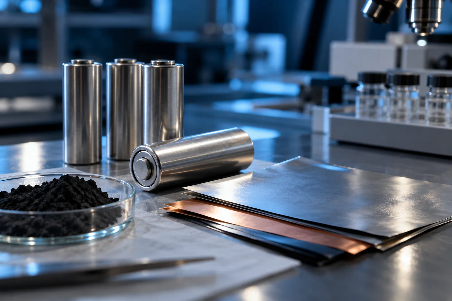
Chiplet designs build a processor from several smaller silicon dies joined by advanced packaging, which can make large designs easier to manufacture and reuse. The joins add cost, heat and capacity limits, and standards such as UCIe and packaging routes from TSMC and Intel are moving the approach into commercial products.
Distributed fibre-optic sensing
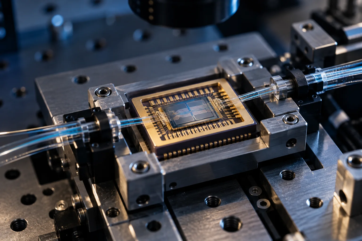
Distributed fibre-optic sensing turns an ordinary optical fibre into a line of thousands of sensing points by reading the light scattered back along it. It can detect vibration and strain along a cable tens of kilometres long, and researchers have used existing telecom and submarine cables to monitor earthquakes and seismic activity.
Extreme ultraviolet (EUV) lithography
Extreme ultraviolet (EUV) lithography prints the finest features on the most advanced chips, using 13.5 nm light made from tin plasma and optics built by ASML, which is the only maker of these machines. Intel reports that High-NA systems are in high-volume manufacturing for a subset of processors at one chipmaker, but cost, source power and a single supplier remain the main limits.
Hollow-core optical fibre
Hollow-core optical fibre guides light through a central air channel instead of solid glass, which can mean lower loss and lower delay per kilometre. A 2025 research paper reported a measured loss of 0.091 dB/km, and Microsoft says the technology is already in use in some Azure regions, but it is not yet a proven commercial product at scale.
Hyperspectral imaging
Hyperspectral imaging records the light reaching each point in hundreds of narrow wavelength bands, so it can separate materials that look the same to a normal colour camera. Two hyperspectral Earth-observation satellites are in orbit and food-sorting systems have been tested on industrial lines, while crop disease detection and medical diagnosis are still mostly at research stage.
Laser communication links
Laser communication links send data as modulated infrared light between spacecraft, aircraft and ground stations, instead of radio waves. NASA has shown 200 Gbps from a small satellite to the ground and 267 Mbps from deep space, but clouds and very precise pointing remain the main practical limits.
Laser-written glass data storage
Laser-written glass data storage encodes information as tiny marks inside blocks of glass using femtosecond lasers. Microsoft's 2026 Nature paper reports a system that could hold about 4.8 TB on a 120 mm square glass plate, but the lifetime claims of more than 10,000 years rest on accelerated tests and extrapolation, and no commercial product has been announced.
Li-Fi (light-based wireless networking)
Li-Fi sends data by rapidly switching the light from LEDs or lasers, and the IEEE 802.11bb light-communications standard was approved in 2023. Single-emitter laboratory links have exceeded 9 Gb/s over short distances, but the link needs an unobstructed path, and the uplink from small devices remains a design challenge.
Metasurface optics and flat lenses
Metasurfaces are flat layers patterned with structures smaller than the wavelength of light, which bend and focus light in place of curved glass. Research metalenses have now focused the full visible spectrum to one point, but they are research prototypes, and the sources reviewed here give no verified commercial performance figures.
MicroLED displays
MicroLED displays use arrays of microscopic light-emitting diodes as pixels, so each pixel makes its own light. Laboratory results are promising, but moving millions of tiny chips onto a screen with near-zero defects is the main manufacturing barrier, and the technology has so far reached commercial use mainly in large commercial and professional screens.
Optical interconnects and co-packaged optics
Optical interconnects carry data between chips, switches and racks as light rather than electrical current. Co-packaged optics (CPO) places the optical engines inside the same package as the switch or processor, which shortens the electrical links and may reduce power per bit, but the approach is still in early industrial use.
Photonic computing for AI
Photonic computing uses light, rather than electrical signals, to carry out some of the matrix calculations used in AI. Laboratory chips have run small neural networks and a packaged optical accelerator, but the sources reviewed here do not show that photonic chips outperform electronic hardware on real AI workloads.
Photonic integrated circuits
Photonic integrated circuits put lasers, waveguides, modulators and detectors on a single chip so that light, rather than only electricity, carries and processes signals. Silicon photonics has established foundry access, and Broadcom's 2025 co-packaged optics switch uses silicon photonics engines. Thin-film lithium niobate and indium phosphide serve other functions.
Photonic quantum computers
Photonic quantum computers use single particles of light, photons, as qubits and move them through chips and optical fibre. Companies such as Xanadu, PsiQuantum and Quandela have reported working prototypes and chip-level component results, but photon loss is a major barrier to building error-corrected machines at useful scale.
Quantum key distribution
Quantum key distribution (QKD) lets two parties agree a shared secret key using quantum states of light, so that interception can be detected. Field experiments have reached over 1,000 km of fibre and a satellite-to-ground link, but the UK National Cyber Security Centre does not endorse QKD for government or military use.
Quantum memories
Quantum memories are devices that take a quantum state carried by light, hold it, and release it later. A solid-state memory has reached efficiency of up to 69%, and nuclear spin coherence has been measured for hours, but the best results come from separate experiments, and none of the sources reviewed shows a memory that combines long storage, high efficiency and high fidelity in one device.
Quantum repeaters and quantum networks
Quantum repeaters use quantum memories to store entanglement while it is passed along a chain of links, so that entanglement can reach beyond the distance that a single optical fibre allows. Small laboratory networks with two or three nodes, some linked over deployed fibre, have now been reported, but the sources reviewed here show no repeater chain yet working over long distances.
Solid-state lidar
Solid-state lidar measures distance with laser light using few or no large moving parts. It uses flash illumination, optical phased arrays or chip-scale FMCW. Chip results have been shown in the laboratory, but independent evidence of long-range, low-cost sensors in production is still limited.
Thin-film lithium niobate photonics
Thin-film lithium niobate is a chip platform in which light is guided and switched in a thin layer of an electro-optic crystal. Laboratory modulators have carried data at up to 210 gigabits per second, and the same platform makes frequency combs, but commercial foundry supply is only starting and most company performance figures have not been independently checked.
Two-photon lithography and nanoscale 3D printing
Two-photon lithography uses a focused laser to harden a liquid resin only at the tiny point where two photons are absorbed together. This lets it print three-dimensional structures with features smaller than the laser's wavelength, but it remains mainly a research tool because suitable resins are scarce and the method has not been scaled to commercial volumes.
How far away are we?
A probe to another star
Science demonstrated · 1 of 8 steps done
A quantum internet
Engineering prototypes · 4 of 7 steps done

Cheap lidar in every car
Scaling up · 5 of 9 steps done
Chips made with the next generation of EUV machines
Pilots · 5 of 9 steps done
Computers that calculate with light in data centres
Engineering prototypes · 5 of 8 steps done
Internet cables that carry light through air
Pilots · 2 of 6 steps done
Laser internet between space and the ground
Pilots · 5 of 7 steps done
MicroLED screens in everyday devices
Pilots · 1 of 5 steps done
Printing features smaller than a cell
Pilots · 4 of 8 steps done
Storing quantum information long enough for a quantum internet
Engineering prototypes · 5 of 7 steps done
Breakthroughs
Grayscale projection two-photon lithography reports 55 nm nanowires and 1.7 billion voxels per second
Kim and Saha (Georgia Institute of Technology) report grayscale projection two-photon lithography. Despite using a binary mask, the method projects more than 15,000 focal spots, each with independently tunable intensity. The abstract says the authors demonstrated printing nanowires as thin as 55 nm and achieved rates of 1.7 billion voxels per second and 215 mm³ per hour. The abstract also describes rapid 3D printing with a single femtosecond pulse per layer. The abstract does not give the resin, laser wavelength or specific exposure parameters.
Experimental 400 Gb/s single-fibre transceiver built on a SiON optical interposer
The arXiv preprint reports an experimentally evaluated 400 Gb/s single-fibre optical transceiver built from 2.5D co-packaged optical I/O chipsets on a SiON/Si interposer. The abstract reports clear eye diagrams and high receiver sensitivity, but gives no sensitivity value or test conditions. The design uses wavelength-division multiplexing, flip-chip integrated InP electro-absorption modulated lasers and photodetectors, and is described as polarisation-insensitive with high fabrication tolerance.
Metalens arrays split one femtosecond laser into more than 120,000 focal spots for parallel nanoscale 3D printing
The team split a femtosecond laser into more than 120,000 focal spots using arrays of metalenses. A spatial light modulator adjusts the intensity of each spot in real time. The spots wrote 3D structures at the same time over centimetre-scale areas, and the reported minimum feature size was 113 nm in the demonstrated structures. The Lawrence Livermore National Laboratory (LLNL) release states that the throughput is more than a thousand times that of commercial systems. The work also printed 16 different microscopic chess openings and produced tens of millions of micro-particles per day.
Polymer and water lenses shaped by surface tension on ISS, preprint reports
A preprint (arXiv:2510.06474, posted 7 October 2025) reports two Fluidic Shaping experiments on the International Space Station during the Ax-1 mission. Fluidic Shaping uses surface tension in microgravity to form optical components from liquid. In the first, centimetre-scale polymer lenses were formed and cured with UV light; the abstract reports sub-nanometric surface smoothness. In the second, a 172 mm diameter water lens was deployed, and image tests showed basic optical function. The abstract also reports that some polymer lenses showed unexpected thermo-chemical deformation.
Hollow-core fibre loss measured below 0.1 dB/km in 2025 Nature Photonics paper
Researchers led by Marco Petrovich and Francesco Poletti reported a measured loss of 0.091 dB/km at 1550 nm for an antiresonant hollow-core fibre, in which light is guided through an air channel rather than solid glass. The preprint abstract says loss stayed below 0.2 dB/km across a 66 THz window, compared with 0.14 dB/km and 26 THz for existing technology. The peer-reviewed version appeared in Nature Photonics under the title 'Broadband optical fibre with an attenuation lower than 0.1 decibel per kilometre'.
Diffractive photonic processor reports 1,024-size matrix multiplication with 10^-6 mean error
The authors report a reconfigurable diffractive tensor processor, the diffractive tensorized unit, that performs arbitrary matrix multiplication at size 1,024 with a mean absolute error of 10^-6. They also report competitive accuracy on natural-language-generation and cross-modal-recognition tasks, and a 1,000-fold improvement in computing throughput over conventional electronic processors in their own comparison.
Twin-field quantum key distribution runs over a 254 km commercial telecom network at 110 bits per second
Pittaluga and colleagues report implementing the coherence-based twin-field QKD protocol over a 254 km commercial telecom network, achieving encryption key distribution at 110 bits per second. The accessible abstract does not give the link endpoints, the cooling or detector method, or the network operator, so the record does not state them.
An integrated photonic accelerator with more than 16,000 components reduces computation time for Ising-problem solvers
Hua and colleagues report a large-scale integrated photonic accelerator with more than 16,000 photonic components, built to perform linear matrix multiply-accumulate operations at up to 1 GHz, with about 3 ns latency per cycle. The authors co-integrated electronic logic, memory and control chips with the photonics using 2.5D hybrid advanced packaging. They report that the low latency reduces computation time for heuristic solvers of hard Ising problems.
Photonic processor runs ResNet, BERT and an Atari reinforcement learning agent
Lightmatter researchers described a photonic AI processor that executed full models, including ResNet, BERT and the DeepMind Atari deep reinforcement learning algorithm, and reported near-electronic precision for many of these workloads.
Xanadu reports Aurora, a networked photonic quantum computer built from 35 chips
Xanadu announced Aurora, a modular photonic quantum computer built from 35 photonic chips, with 12 qubits and about 13 km of fibre optics in total, described as operating at room temperature. The company says the results were published in Nature and quantified optical loss tolerances, but its announcement gives no numerical loss figure.
Coloured-resist flat lenses focus 550 nm light to a 1.1 µm spot without etching
Flat Fresnel zone plate lenses were patterned from coloured photoresist on 8-inch glass wafers using an i-line stepper, with no etching step. At a 550 nm design and test wavelength, they focused light to a spot about 1.1 µm in diameter. Measured focusing efficiency was 7.2%, counted within 3 times the full width at half maximum. Simulation gave 7.3%. The lenses imaged features down to 1.1 µm on a USAF 1951 target.
NASA's deep-space laser test reached 267 Mbps, falling as distance grew
NASA's Deep Space Optical Communications (DSOC) experiment, flown on the Psyche spacecraft, reached a system maximum of 267 Mbps when the spacecraft was about 33 million miles (53 million km) from Earth. On 24 June 2024, at about 240 million miles (390 million km), the link sustained 6.25 Mbps with a peak of 8.3 Mbps. The uplink used a 7 kW laser at JPL's Table Mountain facility, and the downlink was received by Caltech's 200-inch Hale Telescope at Palomar Observatory.
Hybrid event and 20 fps camera matches 5,000 fps latency in offline driving detection tests
Gehrig and Scaramuzza pair a 20 fps RGB camera with an event camera in a detector called DAGr. The authors report that the combination matches the perceptual latency of a 5,000 fps camera while using bandwidth close to that of a 45 fps camera. The tests ran on recorded driving data, not on a vehicle in real time.
Etching-free pixel definition gives 10 µm green micro-LEDs 6.48% on-wafer peak efficiency
Research arrays of InGaN green micro-LEDs with 50, 30 and 10 µm pixels were made using selective thermal oxidation, a method that defines pixels without plasma etching. The 10 µm array reached a peak on-wafer external quantum efficiency of about 6.48%, which the main text reports at 0.4 mA. Peak efficiency fell with pixel size (8.02%, 7.79% and 6.48% for 50, 30 and 10 µm at 0.4 mA). Its leakage current density was 1.2 × 10⁻⁶ A/cm² at -10 V after 4 hours of air annealing with a 3.5 µm SiO2 layer. The authors describe this leakage as at a relatively low level compared with micro-LEDs made using conventional plasma etching and dielectric passivation, citing values reported in other studies.